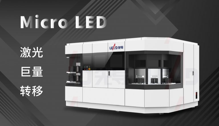
Recently, Micro LED laser mass transfer equipment independently developed by Lead Laser was successfully shipped and entered the process verification stage, becoming one of the few advanced equipment in China to achieve mass transfer, representing the top level of scientific and technological strength in this field.

Micro LED is a new generation of display technology after OLED, which has become more and more sought after by the industry in recent years. Compared with LCD and OLED displays, Micro LED has better resolution and color saturation, lower power consumption, enjoying high application potential in VR/AR, mobile phones, tablets and other fields. However, the development of the massive transfer technology involved in the Micro LED process is extremely difficult, posing as the biggest hurdle in restricting the mass application of Micro LED. Lead Laser has successfully developed laser mass transfer equipment, greatly promoting the rapid development of the Micro LED industry.
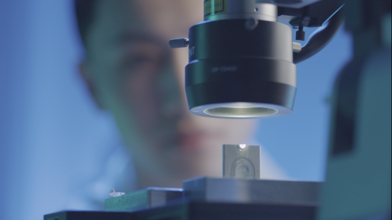
Mass transfer technology is mainly to transfer millions or even tens of millions of micron LED cells to the drive substrate quickly and accurately, and form a good electrical connection and mechanical fixation with the drive circuit. To achieve this, there are multiple technical routes to choose from. Lead Laser chooses the laser transfer method and this method is characterized by the use of laser absorption via material, causing thermal expansion of the interface and thereby causing ablation of the sacrificial layer. In the end, Micro LED is transferred from the original substrate to the receiving substrate. If it is a GaN epitaxial wafer, the GaN buffer layer at the interface will be decomposed into Ga and N2 to achieve the separation and transfer of the chip.

Thanks to its rich experience in automated manufacturing, Lead Laser mass transfer equipment has unique advantages in many aspects such as transfer yield and reliability. According to result of verification, the mass transfer yield of the equipment can reach 99.99% with a transfer accuracy of within ±1um. The equipment itself is design based on Lead Laser‘s engineering language characterized by reasonable structure, good operability. And combined with modular design, different machine structures can be configured to achieve various functional upgrade. Besides, advanced optical technology is adopted to realize fully automatic grain transfer with improved transfer efficiency. For different products, Lead Laser mass transfer equipment is compatible with 2-inch, 4-inch, 6-inch wafers and a variety of load/drive substrates at the same time.
Laser technology is an important tool for precision processing and manufacturing industry. Since 2019, Lead Laser has been continuously exploring the application of lasers in various manufacturing scenarios. In the emerging new display field, Lead Laser equipment shipments account for the industry's leading percentage, and has developed LLO, mass welding, laser repair and other advanced processes.
In the future, Lead Laser will continue to increase R&D and investment in laser equipment; accelerate the arrangement of business in display panels, semiconductors, consumer electronics, new energy, new type of display and other segments; promote the synchronous upgrade of laser and relevant traditional industries, and release full potential of laser in the field of intelligent manufacturing.


